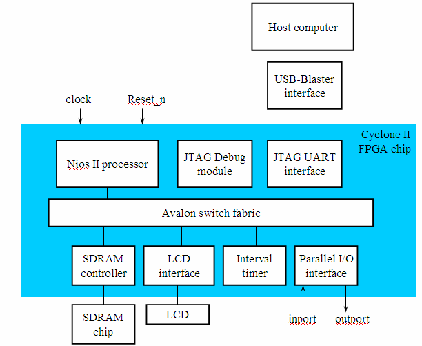
Our second Nios II system uses SDRAM instead of the on-chip memory of the Cyclone II FPGA.

The SDRAM chip on the DE2 board has the capacity of 64 Mbits (8 Mbytes). It is organized as 1M x 16 bits x 4 banks.
sys2, so my top-level module
will be sys2.v
You may download my version of the top-level module from sys2.zip. The module sys2.v uses the DE2 pin names specified in DE2_pin_assignments.csv. It connects the 18 toggle switches to inport and the 32 output bits to the seven-segment displays, suppresssing leading zeros.
processor2 in the dialog box shown
below.
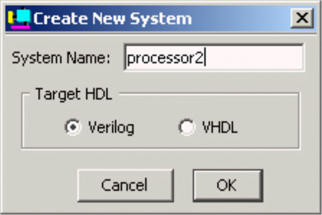
Figure 1. System Creation dialog
Include the following components as shown in Figure 2. Some of the components require additional explanation.
Exit SOPC Builder to complete the rest of the system. You can generate the CPU now or do it later.
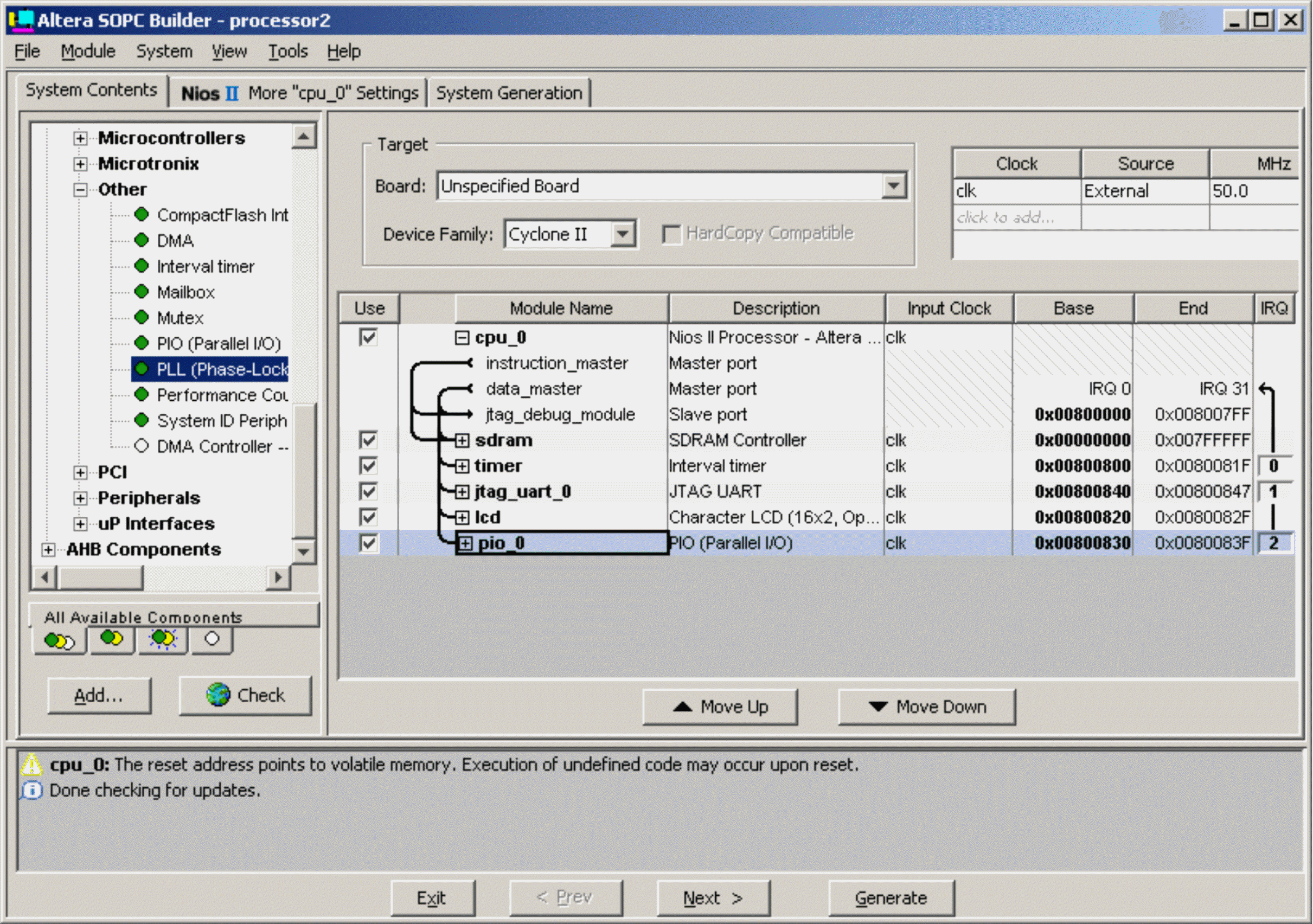
Figure 2. SOPC System Summary
To add the SDRAM, select Avalon
Components >Memory >SDRAM Controller and click Add. A window depicted
in Figure 3 appears. Set the Data Width parameter to 16 bits and leave
the default values for the rest. Uncheck the option to Include a functional memory
model in the system testbench. Click Finish. Now, in the window of
Figure 3, there will be an sdram_0 module added to the design. Since
there is only one SDRAM on the DE2 board, you may rename this
module to simply sdram, by right-clicking on the original
name and selecting rename.
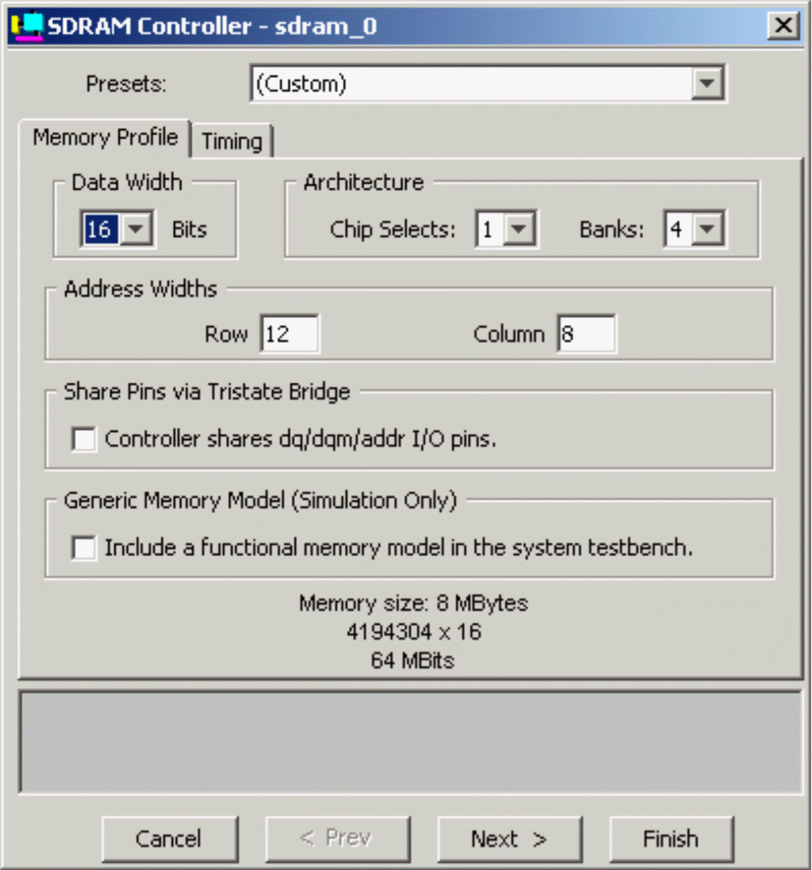
Figure 3. SDRAM Controller
Add a PIO unit as shown in Figure 4. Include 32 bits, both input and output ports. Add support for detecting edge transistions and using them to trigger interrupts.
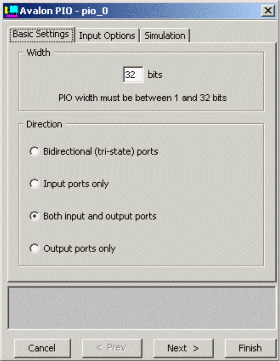
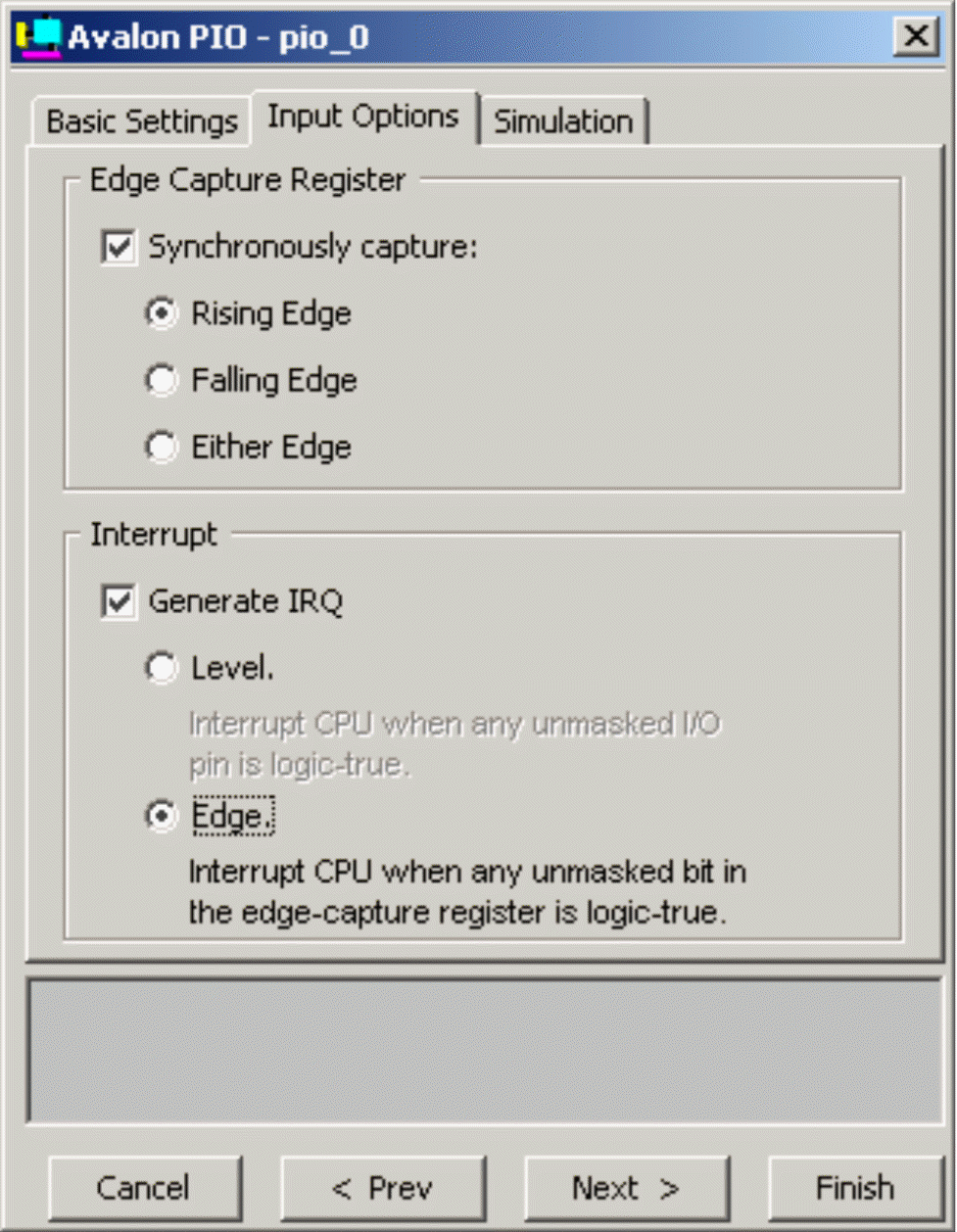
Figure 4. PIO
The clock skew depends on physical characteristics of the DE2 board. For proper operation of the SDRAM chip, it is necessary that its clock signal, DRAM_CLK, leads the Nios II system clock, CLOCK_50, by 3 nanoseconds. This can be accomplished by using a phase-locked loop (PLL) circuit. There exists a Quartus II Megafunction, called ALTPLL, which can be used to generate the desired circuit. The circuit can be created, by using the Quartus II MegaWizard Plug-In Manager, as follows:
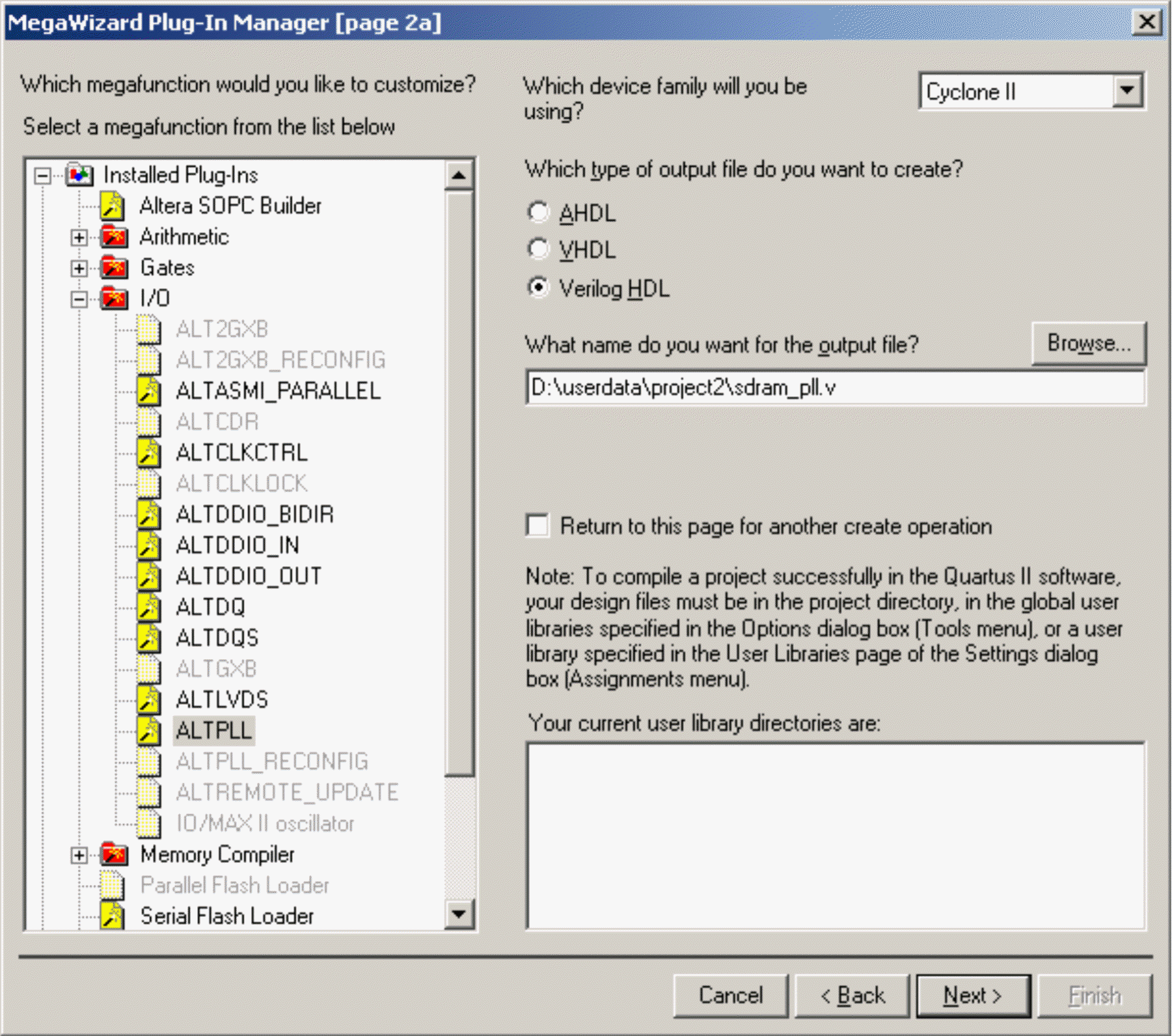
Figure 5. ALTPLL Megafunction
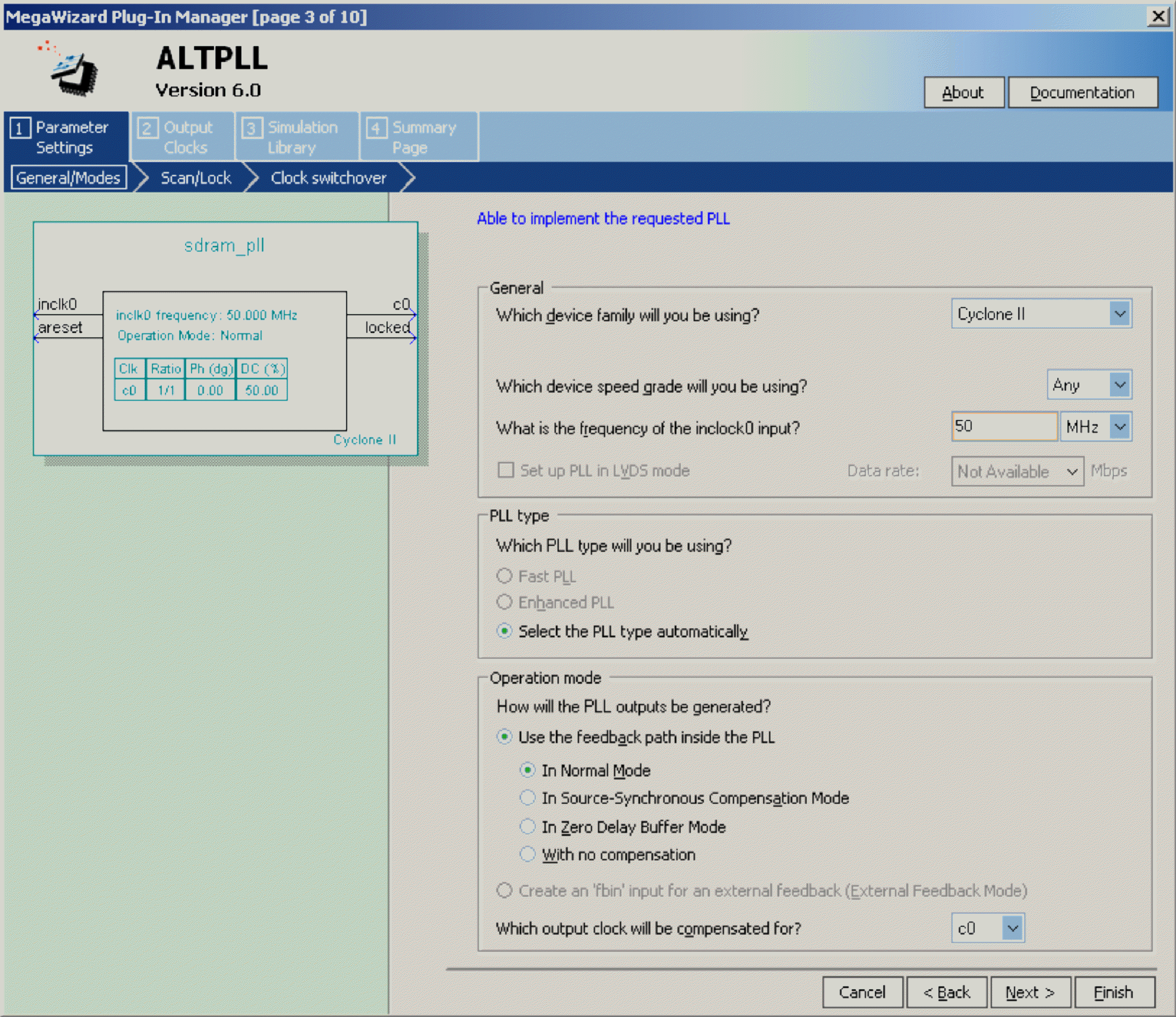
Figure 6. ALTPLL Wizard page 3
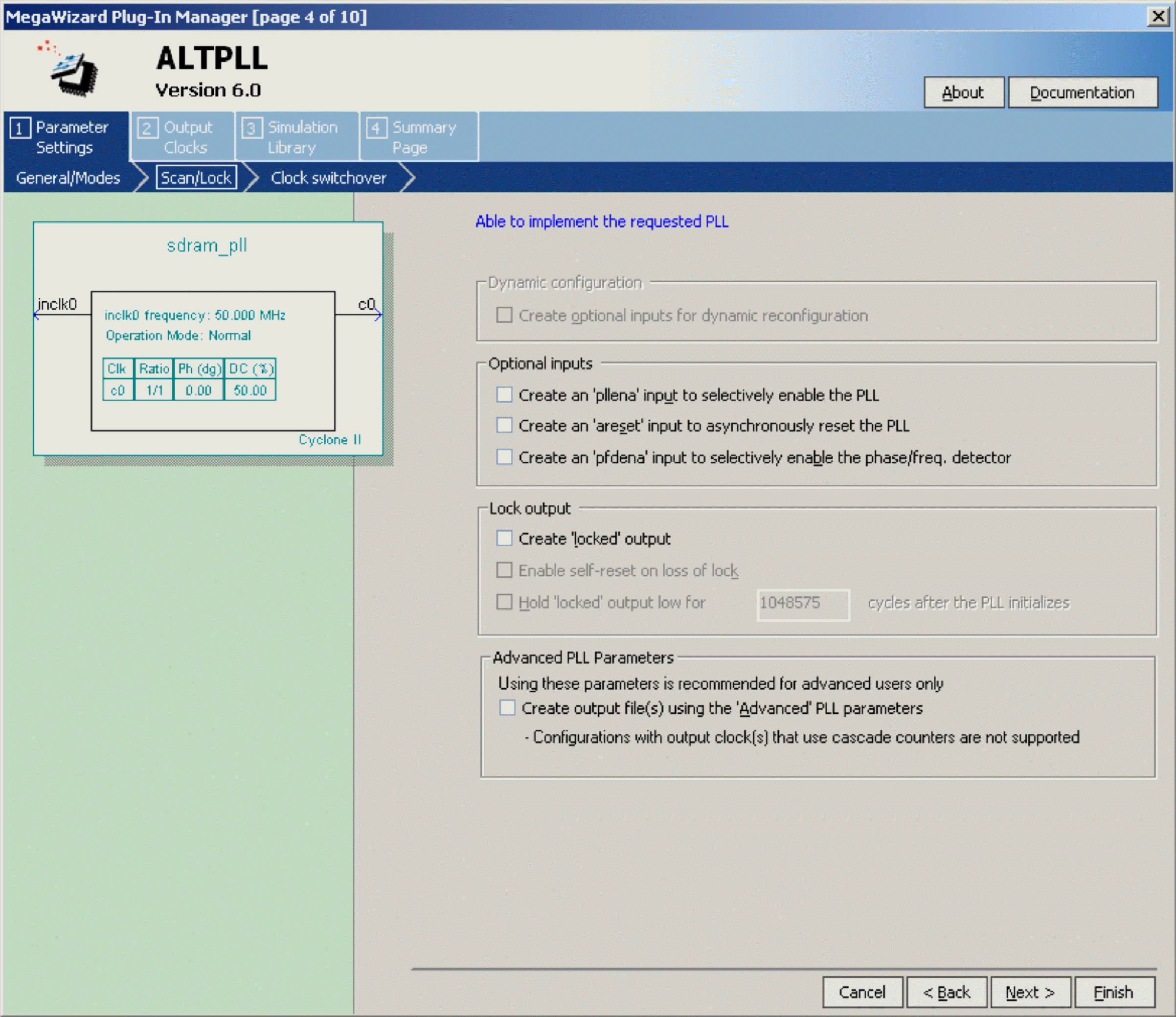
Figure 7. ALTPLL Wizard page 5
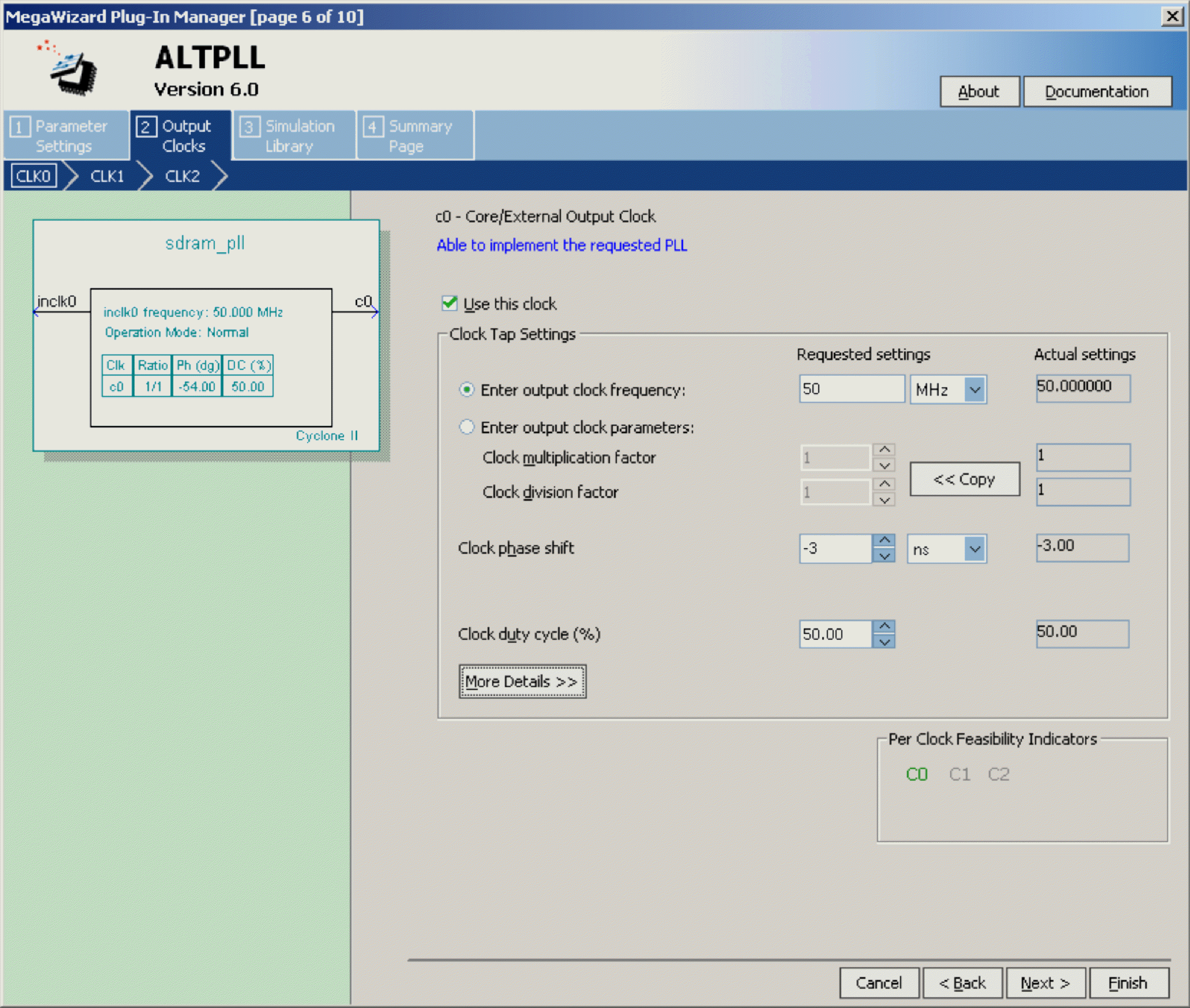
Figure 8. ALTPLL Wizard page 6
The following waveforms show the behavior of altpll megafunction for the chosen set of parameters in design sdram_pll.v. The design sdram_pll.v has Cyclone II FAST pll configured in NORMAL mode The primary clock input to the PLL is INCLK0, with clock period 20000 ps. CLK0 multiply by = 1, CLK0 divide by = 1, CLK0 phase_shift = -3000

Maintained by John Loomis, last updated 20 June 2007