ECE303L Signals and Systems Lab 5
Objectives
- Review properties of operational amplifier.
- Investigate properties of integrator and differentiator circuits.
- Investigate properties of a passband Sallen-Key active filter.
- Investigate the use of frequency sweeps to analyze filter
characteristics.
Background
Download lab5
materials
The pin layout of the LM1458 Dual Operational Amplifier (datasheet) used in
this lab is shown in Figure 1 below.
|
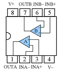
Figure 1. LM1458 Pin Diagram
|
|
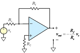
Figure 2. Inverting amplifier
|
Figure 2 shows a simple inverting amplifier circuit that we use to
characterize some properties of the operational amplifier itself.
Results of some measurements using a different operational amplifier are reported
in the link.
Integrator
An ideal (inverting) Integrator can be build using the
schematic in Figure 3 below.
|
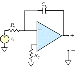
Figure 3. Ideal integrator circuit
|
|
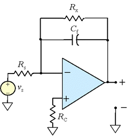
Figure 4. Improved integrator circuit.
|
The ideal integrator suffers from two main limitations. One comes
from the fact that the output voltage of the opamp can not exceed the
supply voltage. The output of the integrator is inversely proportional
to the time constant τ = RsCf. The
larger the time constant τ, the longer it takes to
saturate the integrator. The second limitation is a consequence of the
offset voltage present even for zero input. It may be only a
few millivolts, but it it gets integrated over time it eventually
drives the OpAmp output to saturation. To prevent this from occurring,
a large (1-10 MΩ) resistor Rx is added
in parallel with the capacitor, as shown in Figure 4.
Differentiator
An ideal (inverting) Differentiator can be build using the
schematic in Figure 5 below.
|
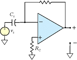
Figure 5. Ideal differentiator circuit
|
|
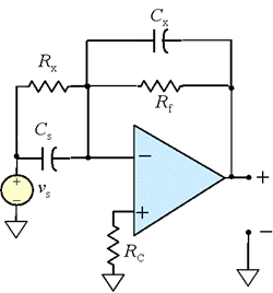
Figure 6. Improved differentiator circuit.
|
Like the integrator before, the ideal differentiator has some
limitations. The output is limited to the supply voltages, and since
the differentiator is a noise-amplifying device, it suffers from
excessive response to high-frequencies. Generally a practical
differentiator is combined with a low-pass filter to smooth the
high-frequency noise effects. Figure 6 shows some possible
modifications to the ideal circuit. A large (over 1 MΩ) resistor
Rx may be inserted in parallel with
Cs and a very small ( 10 pF or less) capacitor
Cx may be inserted in parallel with
Rf.
Sallen-Key Filter
The basic circuit of a band-pass Sallen-Key
filter is shown in Figure 7.
below.
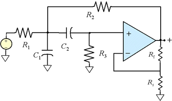
Figure 7. Sallen-Key active filter
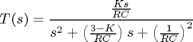
It can be shown that the transfer function of the filter is
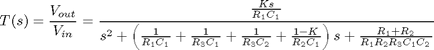
Observe that the transfer function shown in equation above is quite
complex. The analysis can be greatly simplified, however, if all
frequency-determining capacitors are set equal to each other, as well
as all frequency-determining resistors. That is, let
R1 = R2 = R3/2
= R and C1 = C2 =
C.
The original transfer function then simplifies to
A second order band-pass transfer function can written in the following standard form
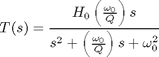
Comparing coefficients of the last two equations, we see that


An example Sallen-Key bandpass filter, analyzed using MATLAB nodal
equations and the symbolic toolkit, is shown the following MATLAB script.
Frequency Sweep
You learned how to set the function generator to do a frequency
sweep in lab
1. It is tempting to analyze an active filter by setting the
function generator to sweep through a frequency range of interest and
see how the output waveform changes.
An attempt to predict the results of such a measurement resulted in
the following MATLAB script. The
results were less than satisfactory. The filter examined was a
passband filter with center frequency of 1200 Hz and 100 Hz bandwidth.
The calculated waveform showed a center frequency of about 1000 Hz and
some unexpected structure in the envelope. Either there is a problem with
the script or the measurement itself is more complicated than
anticipated.
As part of this lab, perform the measurement and report on the
results. See if you can find a problem in the MATLAB script.
Requirements
- Characterize your operational amplifier by doing the following.
- Construct the inverting amplifier circuit shown in Figure 1,
with a gain of -10. Suggested resistances are Rf = 470
kΩ, Rs =
47 kΩ, and RC = 10 kΩ.
- Measure the gain and phase shift from 100 Hz to 100 kHz. Use a
MATLAB script to make the measurements. Plot the results and tabulate
values at decade intervals (100 Hz, 1 kHz, 10 kHz, and 100 kHz).
- Measure the saturation (clipped) peak-to-peak level at 1 kHz. Set
the input so that the ideal output value would be 25 volts
peak-to-peak. Attach an image of the oscilloscope output to the
report.
- Measure the slew rate by using a square-wave at a frequency that
clearly shows slew-limited behavior. Measure the rise and fall times
and the peak-to-peak output voltage. Attach an image of the
oscilloscope output to the report.
- Find the frequency at which the gain drops to 0.707 of its ideal
value. Measure the phase shift at that frequency.
- Ground the input of the OpAmp and measure the output voltage
(offset voltage).
- Build an integrator circuit as shown in Figure 3. Suggested values
are 40-100 kΩ for Rs,
100 nF to 0.01 μF for Cf, and 10-20
kΩ for Rc. Try the ideal circuit first
and determine the effects of offset voltage by measuring the rate
of change of the output voltage with the input grounded. You may
need to short the integrating capacitor before starting your
measurement. If the output is unstable, insert a large resistor in parallel
with the capacitor, as shown in Figure 4. Then characterize the system
as follows:
- Measure the frequency response (magnitude and phase) of the
system. Compare the results to theoretical expectations.
- Show that the output of the integrator is a triangle wave if the
input is a square wave. Capture a demonstration oscilloscope trace
showing the frequency and peak-to-peak magnitude of input and output.
- Capture an oscilloscope image showing the output and input of the
integrator if the input is a noise signal
from the signal generator.
- Build an differentiator circuit as shown in Figure 5. Suggested values
are 40-100 kΩ for Rf,
100 nF to 0.01 μF for Cs, and 10-20
kΩ for Rc. Try the ideal circuit first
and determine the effects of noise by evaluating the output for a
variety of input signals. If the output noise levels are
unacceptable, modify the circuit by the addition of
Rx and/or Cx, as shown in Figure
6. Then characterize the system as follows:
- Measure the frequency response (magnitude and phase) of the
system. Compare the results to theoretical expectations.
- Show that the output of the differentiator is a square wave if the
input is a triangle wave. Capture a demonstration oscilloscope trace
showing the frequency and peak-to-peak magnitude of input and output.
- Capture an oscilloscope image showing the output and input of the
differentiator if the input is a noise signal
from the signal generator.
- Build a Sallen-Key circuit as shown in Figure 7. Design the
filter for a center frequency of 1500 Hz and a Q of 4. Keep
resistor values above 1 kΩ and capacitance values above 100 pF.
Then characterize the system as follows:
- Measure the frequency response (magnitude and phase) of the
system. Compare the results to theoretical expectations.
- Calculate the observed values of gain, center frequency, and Q.
- Capture an oscilloscope image showing the output and input of the
filter if the input is a noise signal
from the signal generator.
- Simulate your passband filter in SPICE and compare the results
to your measured frequency response above. Adjust the circuit
parameters of your SPICE model to match the measured values of your
circuit components.
- Capture an oscilloscope image showing the input and output of
the filter above with the function generator set to sweep from 1 kHz
to 2 kHz, assuming your passband filter is centered at 1500 Hz.
Discuss the resulting image. Does the modulated sweep have its peak
value at a time for which the input is the center frequency of the
filter? Is the bandwidth of the modulated sweep what you expected? Are
there any unexpected structures?
Maintained by John Loomis,
last updated 25 October 2010