
An equivalent circuit for a phototransistor consists of a photodiode feeding its output photocurrent into the base of a small signal transistor. Based on this model it is not surprising that phototransistors display some of the characteristics of both types of devices.
The output of a phototransistor is dependent upon the wavelength of incident light. These devices respond to light over a broad range of wavelengths from the near UV, through the visible and into the near IR part of the spectrum. Unless optical filters are used, the peak spectral response is in the near IR at approximately 840 nm. The peak response is at a somewhat shorter wavelength than that of a typical photodiode. This is because the diffused junctions of a phototransistor are formed in epitaxial rather than crystal grown silicon wafers.
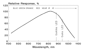
Phototransistors will respond to fluorescent or incandescent light sources but display better optical coupling efficiencies when matched with IR LEDs. Standard IR LEDs are GaAs (940 nm) and GaAlAs (880 nm).
For a given light source illumination level, the output of a phototransistor is defined by the area of the exposed collector-base junction and the dc current gain of the transistor. The collector-base junction of the phototransistor functions as a photodiode generating a photocurrent which is fed into the base of the transistor section. Thus, like the case for a photodiode, doubling the size of the base region doubles the amount of generated base photocurrent. This photocurrent (IP) then gets amplified by the dc current gain of the transistor. For the case where no external base drive current is applied:
IC = hFE (IP)
where:
IC = collector current
hFE = DC current gain
IP = photocurrent
As is the case with signal transistors, hFE is not a constant but varies with base drive, bias voltage and temperature. At low light levels the gain starts out small but increases with increasing light (or base drive) until a peak is reached. As the light level is further increased the gain of the phototransistor starts to decrease.
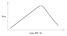
Transistor Gain vs Light Intensity
HFE will also increase with increasing values for VCE. The current -voltage characteristics of a typical transistor will demonstrate this effect.
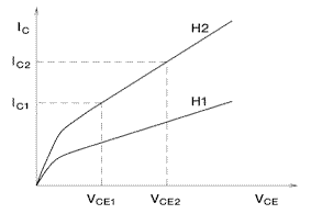
Current vs Voltage Curves
For a constant base drive the curve shows a positive slope with increasing voltage. It is clear that the current gain at collector-emitter voltage VCE2 is greater than the current gain at VCE1. The current gain will also increase with increasing temperature.
Unlike a photodiode whose output is linear with respect to incident light over 7 to 9 decades of light intensity, the collector current (IC) of a phototransistor is linear for only 3 to 4 decades of illumination. The prime reason for this limitation is that the dc gain (hFE) of the phototransistor is a function of collector current (IC) which in turn is determined by the base drive. The base drive may be in the form of a base drive current of incident light.
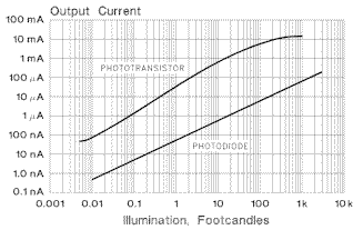
Photodetector Relative Linearity
While photodiodes are the detector of choice when linear output versus light intensity is extremely important, as in light intensity measuring equipment, the phototransistor comes into its own when the application requires a photodetector to act like a switch. When light is present, a phototransistor or photodarlington can be considered "on", a condition during which they are capable of sinking a fair amount of current. When the light is removed these photodetectors enter an "off" state and function electrically as open switches. How well phototransistors function as switches are covered in the next few sections.
By definition, saturation is the condition in which both the emitter-base and the collector-base junctions of a phototransistor become forward biased. From a practical standpoint the collector-emitter saturation voltage, VCE(SAT), is the parameter which indicates how closely the photodetector approximates a closed switch. This is because VCE(SAT) is the voltage dropped across the detector when it is in its "on" state.
VCE(SAT) is usually given as the maximum collector-emitter voltage allowed at a given light intensity and for a specified value of collector current. EG&G Optoelectronics tests their detectors for VCE(SAT) at a light level of 400 fc and with 1 mA of collector current flowing through the device. Stock phototransistors are selected according to a set of specifications where VCE(SAT) can range from 0.25 V (max) to 0.55 V (max) depending on the device.
When the phototransistor is placed in the dark and a voltage is applied from collector to emitter, a certain amount of current will flow. This current is called the dark current (ID). This current consists of the leakage current of the collector-base junction multiplied by the dc current gain of the transistor. The presence of this current prevents the phototransistor from being considered completely "off", or being an ideal "open" switch.
The dark current is specified as the maximum collector current permitted to flow at a given collector-emitter test voltage. The dark current is a function of the value of the applied collector-emitter voltage and ambient temperature.
EG&G Optoelectronics stock phototransistors and photodarlingtons are tested at a VCE applied voltage of either 5 V, 10 V or 20 V depending on the device. Phototransistors are tested to dark current limits which range from 10 nA to 100 nA.
Dark current is temperature dependent, increasing with increasing temperature. It is usually specified at 25°C.
Phototransistors must be properly biased in order to operate. However, when voltages are applied to the phototransistor, care must be taken not to exceed the collector-emitter breakdown voltage (VBRCEO) or the emitter-collector breakdown voltage (VBRECO). Exceeding the breakdown voltages cause permanent damage to the phototransistor. Typical values for VBRCEO range from 20 V to 50 V. Typical values for VBRECO range from 4 V to 6 V. The breakdown voltages are 100% screened parameters.
The speed of response of a phototransistor is dominated almost totally by the capacitance of the collector-base junction and the value of the load resistance. These dominate due to the Miller Effect which multiplies the value of the RC time constant by the current gain of the phototransistor. This leads to the general rule that for devices with the same active area, the higher the gain of the photodetector, the slower will be its speed of response.
A phototransistor takes a certain amount of time to respond to sudden changes in light intensity. This response time is usually expressed by the rise time (tR) and fall time (tF) of the detector where:
tR - The time required for the output to rise from 10% to 90% of its on-state value.
tF - The time required for the output to fall from 90% to 10% of its on-state value.
As long as the light source driving the phototransistor is not intense enough to cause optical saturation, characterized by the storage of excessive amounts of charge carriers in the base region, risetime equals falltime. If optical saturation occurs, tF can become much larger than tR.
EG&G Optoelectronics tests the tR and tF of its phototransistors and photodarlingtons at an IC = 1.0 mA and with a 100 ohm load resistor in series with the detector. Phototransistors display tR and tF times in a range of 1 µsec to 10 µsec. The tR and tF of photodarlingtons typically lie between 30 µsec and 250 µsec.
Each application is a unique combination of circuit requirements, light intensity levels, wavelengths, operating environment and cost considerations. EG&G Optoelectronics offers a broad range of catalog phototransistors and photodarlingtons to help you with these design tradeoffs.
The charts presented below are intended to give some general guidelines and tradeoffs for selecting the proper detector for your application.
| Size of Detector Chip | ||
| Small Size | Parameter | Large Size |
| Lower | Sensitivity | Higher |
| Faster | Speed of Response | Slower |
| Lower | Dark Current | Higher |
| Lower | Cost | Higher |
| Gain (HFE) | ||
| Low Gain | Parameter | High Gain |
| Lower | Sensitivity | Higher |
| Faster | Speed of Response | Slower |
| Lower | Dark Current | Higher |
| Smaller | Temp. Coef. | Larger |
| Lower | Cost | Higher |
For a copy of the original data sheet, or to send comments,
E-Mail us at: eod@egginc.com
Or call us at 1-800-775-OPTO (6786).
Copyright© 1997 EG&G, Inc. Legal Notices
45 William Street, Wellesley, Massachusetts, U.S.A.
All Rights Reserved.