Microelectronics Assignment 4
Your report should be a Microsoft Word document or PDF.
Supplemental computer files associated with the
assignment (SPICE, spreadsheets, etc.) should be referenced in the
main document and included in your submission, organized in some
appropriate manner.
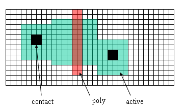
- The diagram below shows a transistor (poly over n+)
with a grid spacing of one λ square. Assume a process with
λ = 0.3 µm. Find the
transistor parameters (W, L, AD, PD, AS, PS, NRS, NRD). Assume the
drain is the active area on the right.

- Show the netlist from the NMOS_IV transistor layout obtained
in Assignment 3. Verify the values of AD, AS, PD, and PS using the
dimensions of the source and drain. See example done in class.
- Given the following information from an NMOS characteristic
curve (VGS = 5 Volts):
| VDS (V) | ID (µA)
|
| 2.1 | 237.85
|
| 4.5 | 326.76
|
| 5.0 | 328.76
|
You may find the following formula useful:

- Find the transconductance k and channel modulation
λ for the simple (level 1) model that match the measured
values in the saturation region of
the table above. VT = 0.8 V.
- Find the effective resistance of the transistor.
- Calculate the current ID at VDS = 4 V for the
level 1 model.
- Work through tutorial 3 (see link below). Your report should
include layout figures, schematic figures, and a report of Spice
analysis.
Tutorial
3 – Design, layout, and simulation of a CMOS inverter – electric_tutorial_3_video.wmv
(27:45)
- Design an inverter with the NMOS transistor sized 6x2 (WxL), and the
PMOS transistor sized so that the switch point is close to 2.5 V. Show
a diagram of the resulting circuit and a copy of the netlist. This
inverter should have ports and power node connections and an external
symbol representation - like the example we showed in class.
Maintained by John
Loomis, last updated 10 February 2014

