Microelectronics Assignment 7
Document your work in a Microsoft Word document or PDF.
Show netlists for all Spice calculations.
You must submit your JELIB files and SPICE
schematics and other associated files.
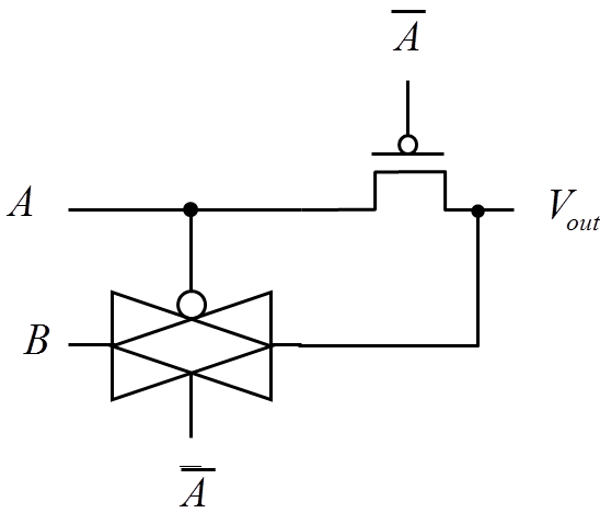
- The circuit below is a TG-based OR gate (See Baker figure 13.11). Generate a symbol and circuit in LTSpice for
a transmission gate, and a test circuit to verify the operation of the OR gate. You should
create an OR symbol and circuit and a separate test circuit that instantiates and tests the
OR gate.
- Use MODSIM to verify the behavior of a NOR gate (built from transistor PMOS/NMOS objects).
Follow the example of the NAND gate shown in class.
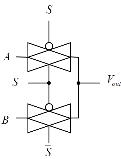
- Layout and test a multiplexer in Electric. Your layout should include the inverter needed
for the complementary control signal. You will need both schematic and layout versions of the
multiplexer and a test circuit in Spice.
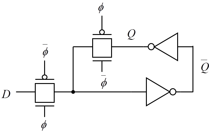
- Layout and test the latch shown below (see Baker figure 13.20). Use Electric for the layout
and LTSpice for the simulation. Include the layout needed for the complementary control circuit.