Introduction to JTAG Boundary Scan
Historically, most Print Circuit Board (PCB) testing was done using
bed-of-nail in-circuit test equipment. Recent advances with VLSI
technology now enable microprocessors and Application Specific Integrated
Circuits (ASICs) to be packaged into fine pitch, high count packages.
These high density devices pose unique manufacturing challenges: such as,
the accessibility of test points and the high cost of test equipment.
In 1985, a group of European companies formed Joint European Test
Action Group (JETAG) to tackle these challenges. It called for
incorporating hardware into standard components (controlled via software),
eliminating the need for sophisticated in-circuit test equipment. By 1988,
the concept gained momentum in North America and several companies formed
the Joint Test Access Group (JTAG) consortium to formalize the idea. In
1990, the Institute of Electrical and Electronic Engineers (IEEE) refined the concept and created the
1149.1 standard, known as IEEE Standard Test Access Port and Boundary Scan
Architecture.
Boundary
scan is a methodology allowing complete controllability and observability
of the boundary pins of a JTAG compatible device via software control.
This capability enables in-circuit testing without the need of bed-of-nail
in-circuit test equipment.
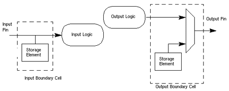
Figure 1. Input and Output Structure for a Boundary Scan Device
(Simplified)
Figure 1 illustrates possible structures for input and output pins
of a JTAG-compliant device. During standard operations, boundary cells are
inactive and allow data to be propagated through the device normally.
During test modes, all input signals are captured for analysis and all
output signals are preset to test down-string devices. The operation of
these scan cells is controlled through the Test Access Port (TAP)
Controller and the instruction register as shown in the following
illustration, Figure
2.
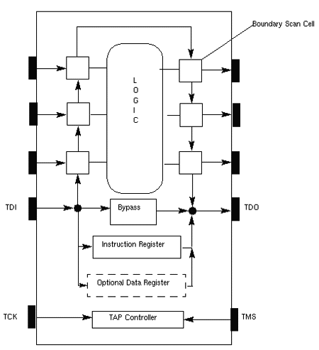
Figure 2. The Boundary Scan Device
The TAP
controller is a state machine (16 possible states) controlling operations
associated with boundary scan cells. The basic operation is controlled
through four pins: Test Clock (TCK), Test Mode Select (TMS), Test Data In
(TDI), and Test Data Out (TDO).
The TCK and TMS pins direct signals between TAP
controller states. The TDI and TDO pins receive the data input and output
signals for the scan chain. Optionally, a fifth pin, TRST, can be
implemented as an asynchronous reset signal to the TAP controller.
Working in
conjunction with the TAP controller is an IR (Instruction Register)
providing which type of test to perform. The 1149.1 Standard requires that
all compliant devices must perform the following three instructions:
1. EXTEST Instruction
This instruction performs a PCB interconnect
test. The EXTEST instruction places an IEEE 1149.1 compliant device into
an external boundary test mode and selects the boundary scan register to
be connected between TDI and TDO. During this instruction, the boundary
scan cells associated with outputs are preloaded with test patterns to
test downstream devices. The input boundary cells are set up to capture
the input data for later analysis.
2. SAMPLE/PRELOAD Instruction
The SAMPLE/PRELOAD instruction
allows an IEEE 1149.1 compliant device to remain in its functional mode
and selects the boundary scan register to be connected between the TDI and
TDO pins. During this instruction, the boundary scan register can be
accessed via a data scan operation, to take a sample of the functional
data entering and leaving the device. This instruction is also used to
preload test data into the boundary-scan register prior to loading an
EXTEST instruction.
3. BYPASS Instruction
A device's boundary scan chain can be
skipped using the BYPASS instruction, allowing the data to pass through
the bypass register. This allows efficient testing of a selected device
without incurring the overhead of traversing through other devices. The
BYPASS instruction allows an IEEE 1149.1 compliant device to remain in a
functional mode and selects the bypass register to be connected between
the TDI and TDO pins. The BYPASS instruction allows serial data to be
transferred through a device from the TDI pin to the TDO pin without
affecting the operation of the device.
In a board
design there usually can be many JTAG compliant devices. All these devices
can be connected together to form a single scan chain as illustrated in Figure
3, "Single Boundary Scan Chain on a Board." Alternatively, multiple
scan chains can be established so parallel checking of devices can be
performed simultaneously.
Figure 3, "Single Boundary Scan Chain on a Board,"
illustrates the on onboard TAP controllers connected to an offboard TAP
control device, such as a personal computer, through a TAP access
connector. The offboard TAP control device can perform different tests
during board manufacturing without the need of bed-of-nail equipment.
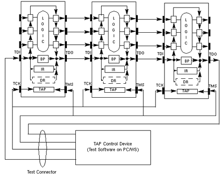
Figure 3. Single Boundary Scan Chain on a Board
One of the first tests that should be performed for a PCB test is
called the infra-structure test. This test is used to determine whether
all the components are installed correctly. This test relies on the fact
that the last two bits of the instruction register (IR) are always ``01''.
By shifting out the IR of each device in the chain, it can be determined
whether the device is properly installed. This is accomplished through
sequencing the TAP controller for IR read.
After the infra-structure test is successful, the board level
interconnect test can begin. This is accomplished through the EXTEST
command. This test can be used to check out ``opens'' and ``shorts'' on
the PCB. The test patterns are preloaded into the output pins of the
driving devices. Then they are propagated to the receiving devices and
captured in the input boundary scan cells. The result can then be shifted
out through the TDO pin for analysis.
These patterns can be generated and analyzed automatically, via
software programs. This feature is normally offered through tools like
Automatic Test Pattern Generation (ATPG) or Boundary Scan Test Pattern
Generation (BTPG).
The
microSPARC-IIep
chip implements the standard 1149.1 boundary scan architecture. It can
be seamlessly integrated with other 1149.1 compliant devices to perform
board level testing. In addition to the standard four-wire (TDI, TDO, TCK,
and TMS) JTAG TAP access port, the microSPARC-IIep also implements the
optional TRST signal line. This allows the on-chip TAP controller to be
reset asynchronously. See Figure 4, "microSPARC-IIep Scan Chain
Organization," for an illustrated description of how the scan chain is
organized in the IIep chip.
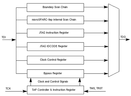
Figure 4. microSPARC-IIep Scan Chain Organization
In addition to the three instructions required by the 1149.1
Standard (see "Required
Instructions"), the microSPARC-IIep also implements other
instructions, see Table
1, "microSPARC-IIep JTAG Commands." These instructions allow different
tests to be performed when the microSPARC-IIep is used as a component in a
board or system environment. See the microSPARC-IIep User's Manual for a
more detailed description.
| Instruction |
IR Value |
Registers |
Function |
| EXTEST |
000000 |
Boundary |
PCB Interconnect test |
| SAMPLE |
000001 |
Boundary |
Sample and data preload |
| BYPASS |
111111 |
Bypass |
Bypass mode |
| SEL_INT_SCAN |
010000 |
Internal Scan Reg. |
Scan IIep internal register |
| SEL_DBG_SCAN |
011111 |
Internal Scan Reg. |
Scan IIep internal register |
| IDCODE |
100000 |
JTAG ID Reg. |
Scan the ID register |
| SEL_CCR |
011110 |
Clock Control Reg. |
Set up clock control |
| CLK_RST |
100000 |
Bypass |
Reset Clock Control |
Board level testing has become more
complex with the increasing use of fine pitch, high pin count devices.
However with the use of boundary scan the implementation of board level
testing is done more efficiently and at lower cost. The microSPARC-IIep
chip fully supports use of the JTAG boundary scan; enabling it to
seamlessly integrate with other IEEE 1149.1 compliant devices on a PCB, as
well as permitting microSPARC-IIep chip to be board level tested without
the PCB expense of complex in-circuit test equipment.
Written by Sun Microelectronics, January 1997
Also in PDF format as wpr-0018-01.pdf (10pp, 147KB)