Download jsim1.zip
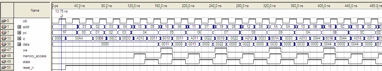
The JSIM1 project demonstrates the ability to read instructions and to
read or write data from the same memory module. Memory accesses are triggered by
latching the address (addr) on the positive edge of the clock.
Data words are transferred to the data vector. A state variable
denotes Instruction Fecth (IFE) and Memory Access (MEM) operations.
The memory_access flag is set when a instruction is either read
or write. The instruction format is:
| 15 | 14 | 13 | 12 | 11 | 10 | 9 | 8 | 7 | 6 | 5 | 4 | 3 | 2 | 1 | 0 |
|---|---|---|---|---|---|---|---|---|---|---|---|---|---|---|---|
| opcode | unused | address | |||||||||||||
An opcode of 4 indicates a store instruction (SW). An opcode of 5 indicates a load instruction (LW). Any other opcode is treated as a NOP.
The first 16 words are instructions
| addr | value | operation | comment |
|---|---|---|---|
| 00 | 00AA | NOP | check for 1 cycle per instruction |
| 01 | 00BB | NOP | |
| 02 | 00CC | NOP | |
| 03 | 00DD | NOP | |
| 04 | A010 | LW 10 | read followed by write 2 cycles per instruction |
| 05 | 8018 | SW 18 | |
| 06 | A011 | LW 11 | |
| 07 | 8019 | SW 19 | |
| 08 | A012 | LW 12 | |
| 09 | 801A | SW 1A | |
| 0A | A013 | LW 13 | |
| 0B | 801B | SW 1B | |
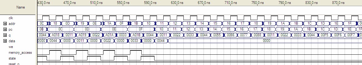
| 0C | A018 | LW 18 | read memory previously written |
| 0D | A019 | LW 19 | |
| 0E | A01A | LW 1A | |
| 0F | A01B | LW 1B |
The last 16 words are data. If interpreted as instructions they would be NOPs.
| addr | value |
|---|---|
| 10 | 11 |
| 11 | 22 |
| 12 | 33 |
| 13 | 44 |
| 14 | 55 |
| 15 | 66 |
| 16 | 77 |
| 17 | 88 |
| 18 | F1 |
| 19 | F2 |
| 1A | F3 |
| 1B | F4 |
| 1C | F5 |
| 1D | F6 |
| 1E | F7 |
| 1F | D8 |
The Verilog code is documented on the jsim1 project page.
The system size is
Total logic elements : 30 / 33,216 ( < 1 % )
    Total combinational functions : 30 / 33,216 ( < 1 % )
    Dedicated logic registers : 22 / 33,216 ( < 1 % )
Total registers : 22
Total memory bits : 512 / 483,840 ( < 1 % )
The memory is 32 words of 16 bits each (32·16 = 512)
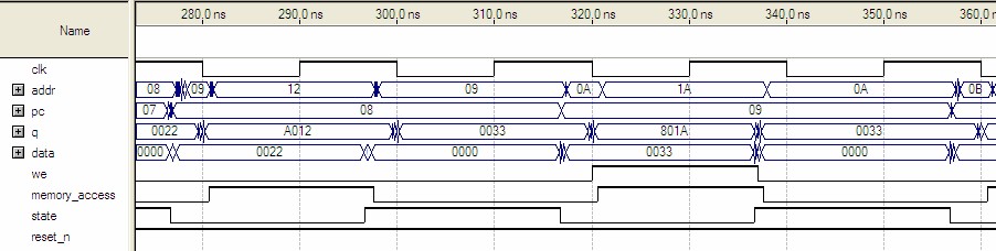
An ASCII text file (with the extension .tbl) that contains a tabular-format list of all input vectors and output logic levels in the current Vector File (.vec) or Vector Waveform File (.vwf). You can save a waveform file as a TBL File by opening the file, choosing Save As, and selecting .tbl as the file type.
The following example shows an excerpt of a sample TBL File generated from a sample VWF File. It corresponds to the region of the simulation output graph shown above. The file has been annotated to show when memory reads were initiated and where the corresponding memory contents were available.
INPUTS clk reset_n;
OUTPUTS addr pc q data we memory_access state;
UNIT ns;
RADIX HEX;
PATTERN
  280.0> 0 1 = 09 08 A022 0022 0 0 0
280.067> 0 1 = 09 08 A032 0022 0 0 0
280.242> 0 1 = 09 08 A012 0022 0 0 0
 280.67> 0 1 = 09 08 A012 0022 0 1 0
280.844> 0 1 = 0B 08 A012 0022 0 1 0
280.879> 0 1 = 0A 08 A012 0022 0 1 0
281.057> 0 1 = 02 08 A012 0022 0 1 0
281.061> 0 1 = 12 08 A012 0022 0 1 0
  290.0> 1 1 = 12 08 A012 0022 0 1 0  latch addr 0x12
296.608> 1 1 = 12 08 A012 0020 0 1 0
 296.72> 1 1 = 12 08 A012 0020 0 1 1
 297.35> 1 1 = 12 08 A012 0000 0 1 1
297.596> 1 1 = 12 08 A012 0000 0 0 1
 297.77> 1 1 = 10 08 A012 0000 0 0 1
297.805> 1 1 = 11 08 A012 0000 0 0 1
297.983> 1 1 = 19 08 A012 0000 0 0 1
297.987> 1 1 = 09 08 A012 0000 0 0 1
299.571> 1 1 = 09 08 2012 0000 0 0 1
299.598> 1 1 = 09 08 0012 0000 0 0 1
299.941> 1 1 = 09 08 0013 0000 0 0 1
  300.0> 0 1 = 09 08 0013 0000 0 0 1
300.242> 0 1 = 09 08 0033 0000 0 0 1  read completed (10.2 ns)
  310.0> 1 1 = 09 08 0033 0000 0 0 1  latch addr 0x09
316.608> 1 1 = 09 08 0033 0002 0 0 1
 316.72> 1 1 = 09 08 0033 0002 0 0 0
316.839> 1 1 = 09 09 0033 0002 0 0 0
316.857> 1 1 = 09 09 0033 0012 0 0 0
316.942> 1 1 = 09 09 0033 0013 0 0 0
317.342> 1 1 = 0B 09 0033 0013 0 0 0
 317.35> 1 1 = 0B 09 0033 0033 0 0 0
317.376> 1 1 = 0A 09 0033 0033 0 0 0
319.571> 1 1 = 0A 09 8033 0033 0 0 0
319.941> 1 1 = 0A 09 8032 0033 0 0 0
  320.0> 0 1 = 0A 09 8032 0033 0 0 0
320.051> 0 1 = 0A 09 803A 0033 0 0 0
320.079> 0 1 = 0A 09 803A 0033 1 0 0
320.242> 0 1 = 0A 09 801A 0033 1 0 0  read completed (10.2 ns)
 320.67> 0 1 = 0A 09 801A 0033 1 1 0
321.061> 0 1 = 1A 09 801A 0033 1 1 0
  330.0> 1 1 = 1A 09 801A 0033 1 1 0  latch addr 0x1A
336.608> 1 1 = 1A 09 801A 0031 1 1 0
For the state machine, only the values at positive clock edges are relevant. We could write a C-program to filter out just the positive edge transistions:
INPUTS clk reset_n;
OUTPUTS addr pc q data we memory_access state;
UNIT ns;
RADIX HEX;
PATTERN
  290.0> 1 1 = 12 08 A012 0022 0 1 0  latch addr 0x12 contents of 0x08 available
  310.0> 1 1 = 09 08 0033 0000 0 0 1  latch addr 0x09 contents of 0x12 available
  330.0> 1 1 = 1A 09 801A 0033 1 1 0  latch addr 0x1A contents of 0x09 available
This filter would simplify the interpretation of the correctness of the state machine by reducing the amount of data to inspect.
Maintained by John Loomis, last updated 17 March 2010